Semiconductor product series
Semiconductor product series
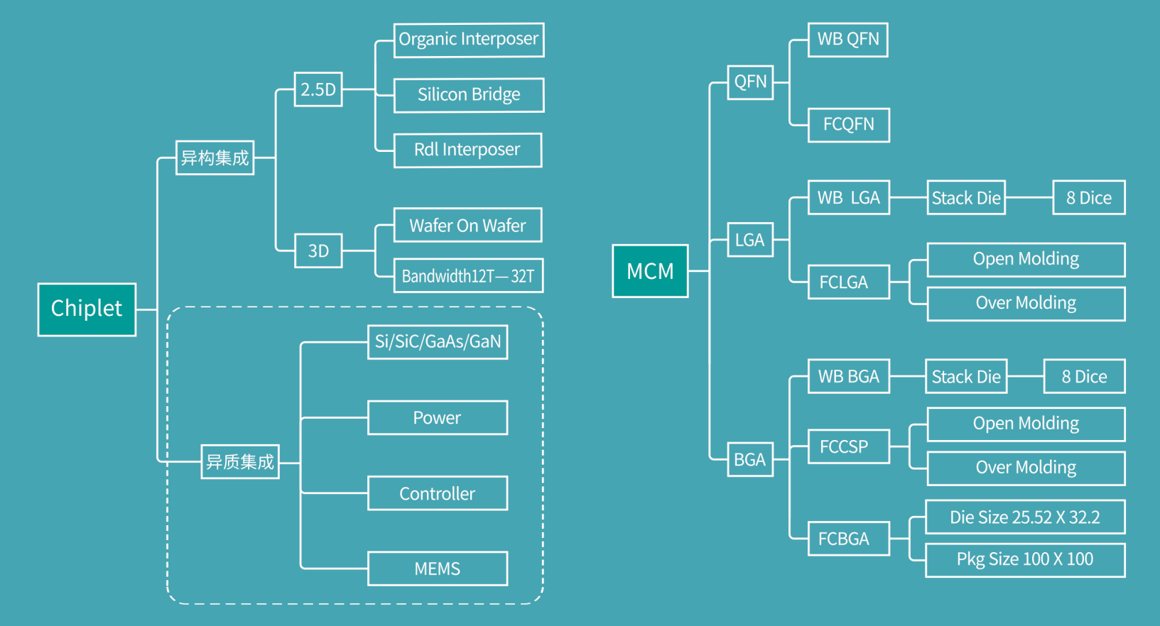
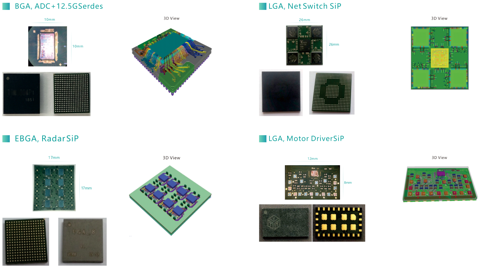
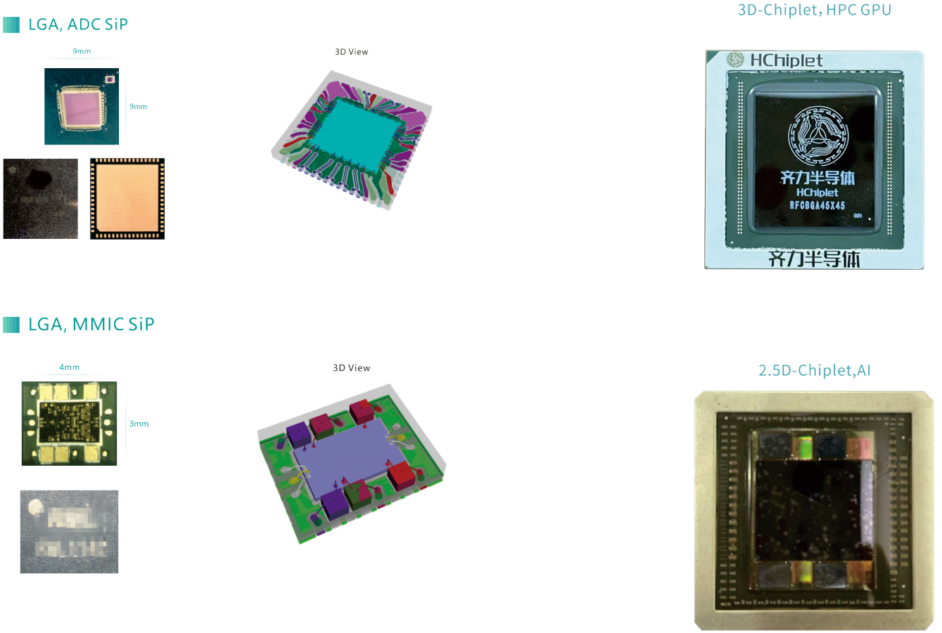
Advanced technology for constructing 3D - Chiplet structures with excellent performance.
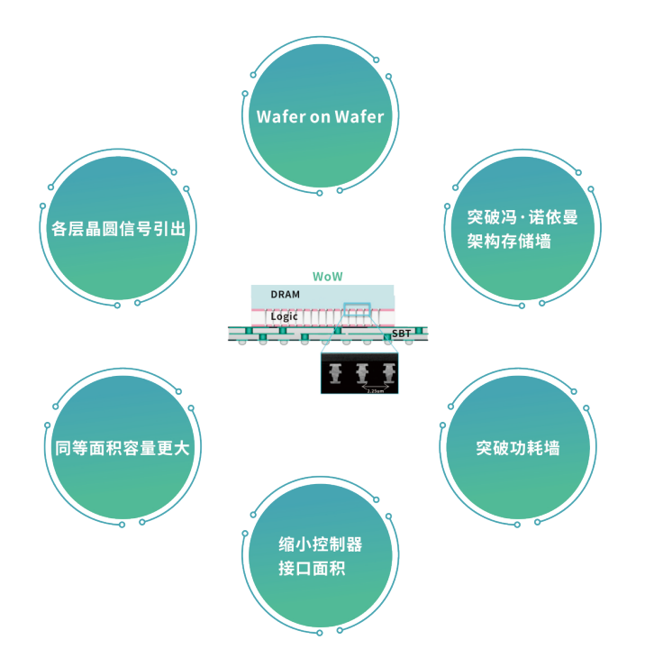
| Implementation scheme of integrated storage and computation based on 3D Chiplet High Bandwidth & High-Speed Interconnection ◆ 3D cross-layer direct connection avoids the problems of 2D routing layout, resulting in lower latency. ◇ TSV (Through-Silicon Vapor) interconnection, and the bandwidth is no longer limited by 2D physical interfaces. ◆ Low Power Consumption ◇ Eliminating the controller saves a significant amount of power. Shorter metal connections lead to even lower power consumption. ◆ Low Cost ◇ The cost-performance ratio of WoW (Wafer-on-Wafer) is higher than that of HBM (High Bandwidth Memory).
Compared with HBM, the in-memory computing integrated chip technology is revolutionary. It inherently has the advantages of high performance, high bandwidth, and high energy efficiency, and can solve the problems of chip performance and energy consumption in the post-Moore's Law era from the underlying architecture. Nowadays, the in-memory computing integrated solutions are attracting more and more attention and are gradually moving from research to commercial applications.
|


